Quick Links
MediaTek announced its first 3nm process chip last week, an unnamed flagship Dimensity SoC that is due to enter mass production in 2024. The news was big, as no other major mobile chip designer - Apple, Qualcomm, or Samsung, has made a 3nm process chip announcement yet.
Apple, however, could announce its first 3nm process mobile processor at its September 12 event, rumoured to make its way into the iPhone 15 Pro models. Before that announcement, let us explain just what a 3nm process chip is and what it would mean for you regarding real-world performance and battery life.
What is a 3nm process chip?
There used to be a simple explanation in the early days of semiconductor processors - one just measured the transistor gate length, starting with micrometres (millionths of a metre, or microns) in the first few decades and progressing to nanometres (billionths of a metre, or nm) as technology matured. As transistor sizes reduced, we saw increased performance, reduced power consumption, and lowered heat generation. It was then relatively easy to say a smaller transistor is better than a larger one, and process node generational improvements were similar among manufacturers.
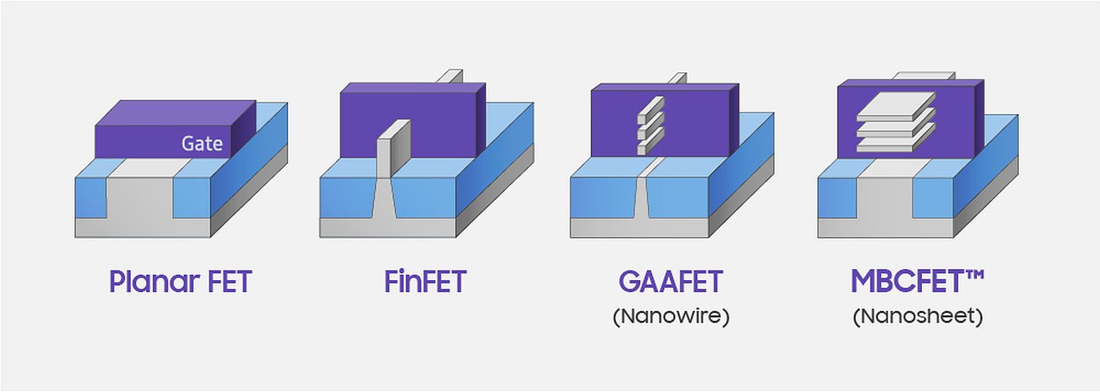
For the past couple of decades, however, it has become a lot more complex to measure performance gains based solely on transistor size, with various proprietary improvements in integrated circuit designs (going from planar transistors to various types of 3D transistors) and fabrication processes effectively decoupling the physical dimensions of a transistor from the process node name. Thus, a 3nm process chip is essentially a marketing term and not directly related to the size of the transistor. Chips from two generations of process nodes (say 5nm and 3nm) made by the same manufacturer should have a smaller overall transistor size on the smaller process node. However, those sizes don't necessarily correspond to the process node name.
Instead, following a processor node scaling plan set by the now-defunct International Technology Roadmap for Semiconductors (ITRS) and then later by the International Roadmap of Devices and Systems (IRDS), microchip manufacturers market each successive generation of their processors by process node names in the roadmap, such as 5nm process and 3nm process nodes. The chips would be expected to follow the IRDS' projections for dimensions like contacted gate pitch and metal pitch but could have even smaller dimensions.
Thus, comparing Intel's 5nm process chip and AMD's 5nm process chip may not be as simple as looking at transistor gate length (or other metrics like metal pitch). There are multiple proposals for new process node nomenclature, such as the GMT (establishing transistor density) and LMC (includes memory and interconnect density) proposals. In the meantime, it would be better to compare the real-world performance of competing chips or compare the performance between different generations of process nodes by the same manufacturer.
In this case, and a great example of the disparity of the process node name from the manufacturer's process - MediaTek announced it had developed its first chip using TSMC's 3nm process. Neither TSMC nor MediaTek have been more precise, stating which of TSMC's proprietary 3nm process nodes is being used - whether N3, N3E, N3S, N3P, or N3X. "MediaTek's first flagship chipset using TSMC's 3nm process is expected to empower smartphones, tablets, intelligent cars, and various other devices starting in the second half of 2024," the release said, and considering that date, it's likely to be the N3S or N3P processes.
The companies have instead detailed generational improvements compared to TSMC's N5 process, which is part of the 5nm process node. It's claimed that TSMC's 3nm process "currently offers as much as [an] 18 percent speed improvement at the same power, or [a] 32 percent power reduction at the same speed, and [an] approximately 60 percent increase in logic density" when compared to the N5 process.
What companies are using 3nm process chips?
So far, beyond MediaTek, no major mobile chip designer has announced a 3nm process chip. This list includes Samsung, Qualcomm, and Apple. To be noted, however, is that Samsung as a foundry has 3nm process chips already in production, but not mobile chips - they are currently being used by cryptocurrency machines.
Qualcomm uses TSMC and Samsung as its foundries, and it is still uncertain which of the two companies would be used for its as-yet-unannounced 3nm process mobile chips.
As we mentioned, Apple is rumoured to launch the 3nm process-based Apple A17 SoC for the iPhone 15 Pro and iPhone 15 Ultra models at its September 12 event. If the reports are true, the company will become the first smartphone/tablet manufacturer with a 3nm process chip in the market in 2023. For several years now, Apple has foregone Samsung as the manufacturer of its A-series processors and chosen TSMC instead.
It's being reported that Apple has booked 90 percent of TSMC's 3nm process production capacity for 2023, which is said to extend to the Apple M3 chip expected to power the MacBook Pro and iPad Pro lineups. However, recent reports suggest the MacBook Pro M3 and iPad Pro M3 won't be launched till next year. The Apple A17 SoC may use TSMC's baseline N3 process.
What will 3nm process chips mean for you?
Smaller transistors, on average, provide improved performance, power consumption, and heat dissipation. Transistor density also increases with smaller transistors. Thus, with smaller distances to travel within and between transistors, electrons take less time to travel within the circuits, improving the processing speed. They would also need less energy to travel these shorter distances, reducing the input power required, and finally, with less movement, cause less energy to be lost as heat.
All this would imply better performance, battery life, and heating all around. This would mean devices with 3nm chips would be faster and last longer than those featuring 5nm or 4nm process chips from the same chip manufacturer.
But of course, there are more contributing factors to these metrics than just the processor or SoC being used. Chip design or architecture, the speed of the memory it is paired with, and other factors, including software, account for the performance of the end device - be it a smartphone, a tablet, or a PC.
Battery life is also affected by the power draw of other components on the device (such as the display) and hardware and software optimisations. And finally, heat dissipation depends a lot on the device's design, and the amount of cooling it is coupled with.
The fact that the latest generation process node chips will be more expensive to produce, and have a lower yield per wafer in the early days of production than previous generations, also implies that they will be limited to the top-end phones and tablets produced by companies. As such, you can expect 3nm process chip smartphones and tablets to be available only in the flagship ranges from each manufacturer for at least another year. The rumour that Apple will only introduce the 3nm process A17 SoC for the iPhone Pro models echoes such a product development decision.
Processor scaling explained
Let's start with the basics: Semiconductors are metalloid materials that possess the properties of both conductors and insulators. Monocrystalline silicon is the most commonly used semiconductor material, and its conductivity is boosted by 'doping' it or adding impurities of other elements to increase its charge-carrying properties. Thin wafers of this material or substrate are grown, and on these, circuits are drawn or built by various physical and chemical processes.
Modern semiconductor processors are constructed with billions of transistors, which form elements of integrated circuits, among other components. These transistors amplify or regulate the flow of electric signals within a circuit and can importantly also act as switches - either on or off, forming the basis of logic processors and memory. For a large part of the history of semiconductor processor manufacturing, the name of a process node (also known as technology node) used to fabricate the chip was designated by the minimum feature size (in nanometres) of a transistor gate length or the minimum linewidth. An example of this would be a 350nm process node.
Let's put that in perspective - a nanometre is a billionth of a metre. With successive generational advances in integrated circuit design and semiconductor fabrication technology, it became possible to build more and more transistors onto a wafer, going from thousands to millions and then billions in a few decades. Process node nomenclature hasn't followed a linear path, though, a problem compounded by the advent of 3D transistors. The number of nanometres used to describe a process node is no longer necessarily related to any physical dimensions of the transistor, such as gate length, metal pitch, or gate pitch.
Instead, manufacturers follow an established IRDS roadmap for successive generational advances in processor scaling, which itself is based on Moore's Law of transistor density doubling every 18-24 months.
Explain the 3nm process like I'm 5
The "3nm process" in a "3nm process chip" refers to the generation of technology used to build the chip. The "3nm", or 3 nanometres, is a marketing term used by the chip maker rather than a description of the technical specifications of the chip - like performance or size. However, 3nm process chips will have smaller transistors when compared to 5nm process chips from the same manufacturer. As transistors become smaller, we can expect performance and energy efficiency increases.


